
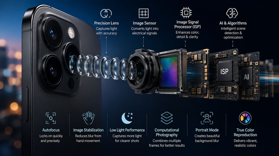
Whether lost in the meadow at the golden hour or crouched in the shadow-cut trenches of a crowded street, we’re all carried away by the same instinct: “lift the phone, frame a face, tap the tiny circle on the screen.”And what follows is much more than a simple click. It’s an engineering vision – an orchestra of optics, sensors, processors, and algorithms that, instantly, turns light into an image. While we obsess over a smile frozen into a portrait, a sunset captured, or the aesthetic perfection of a landscape preserving those happy hours, we remain blissfully oblivious to the intricate engineering process that renders it all flawlessly.
Then what makes us consider this tiny process a grand engineering feat? The answer lies in the extraordinary complexity of a process that begins with something as deceptively simple as light.
A professional DSLR camera can accommodate a lens barrel several centimeters long and a sensor the size of a matchbox. A smartphone camera module, by contrast, must squeeze the same fundamental job, bending light precisely enough to form a sharp image, into a stack barely thicker than a stack of coins. Made from carefully engineered optical elements, the miniature lens controls distortions and other optical imperfections before the light reaches the sensor.
And that is where the magic begins to become engineering.
The journey begins with the lens assembly, usually five to eight plastic or glass elements, each shaped to correct a different optical flaw—chromatic aberration, distortion, and softness at edges. These elements are molded to tolerances measured in microns, then stacked with a precision that was unthinkable in consumer electronics a generation ago. Behind them sits the image sensor, typically a CMOS chip that has become one of the most sophisticated pieces of silicon in the entire phone. It’s not just a light detector; it’s a dense grid of millions of individual photo sites, each capturing photons and converting them into electrical charge, all packed into an area smaller than a fingernail.
Think of it as a remarkably fast digital darkroom operating inside your pocket. It takes the raw information from the sensor and processes it to determine colour, brightness, contrast, sharpness and detail. It may combine information from multiple exposures, correct optical imperfections and reduce noise—all before you have even had time to lower your phone.
Then there is the problem every photographer knows: movement.
Your hand trembles. Your subject moves. The light is poor. A photograph that should have been sharp becomes a blur.
Engineers have spent years finding ways around this. Optical image stabilization, for instance, can physically shift lens elements or the sensor to compensate for tiny movements of the hand. Autofocus systems continuously adjust the optical path to lock onto a subject, often in milliseconds.
The challenge becomes even greater in poor light.
In a dark restaurant or on a dimly lit street, the sensor receives fewer photons, making images susceptible to noise and loss of detail. Modern smartphones increasingly overcome this not simply through better hardware, but through computational photography.
Instead of relying on a single exposure, the phone can capture and analyse multiple frames, align them, and combine useful information from each. Algorithms can then reconstruct an image that is brighter, cleaner, and more detailed than one exposure alone might have produced.
This is where the smartphone camera becomes more than a miniature camera.
It becomes a computational imaging system.
Artificial intelligence and machine learning techniques can recognize faces, skies, landscapes, objects, and scenes, helping the camera decide how an image should be processed. Portrait modes can distinguish a person from the background and simulate the shallow depth of field traditionally associated with larger cameras.
The extraordinary part is not any one of these technologies. It is their miniaturization and coordination.
What makes this genuinely remarkable from an engineering standpoint is not any single innovation but the sheer density of disciplines compressed into a space smaller than a postage stamp. Optical physics, mechanical precision, semiconductor fabrication, thermal management, and machine learning all work in tandem within a power budget measured in milliwatts and a cost budget that still has to fit inside a tiny device. And they have to make this work while consuming limited power, generating manageable amounts of heat, and withstanding the rigors of daily operations—of being carried, dropped, and handled thousands of times.
A misstep in any one layer—a lens element off by microns, a processor too slow to keep pace with the sensor’s data rate —the whole chain collapses into a blurry, noisy failure.
The irony is how we take this complexity for granted. Exceptional engineering is meant to go unnoticed; when a smartphone photo turns out perfectly, it feels obvious, even effortless. Yet behind that simple click lies a massive global web. It relies on optical labs in Japan, microchip factories in South Korea, and coding teams across Silicon Valley and Shenzhen—all of it fires up the exact moment you tap the screen.
So, the next time you tap that familiar camera shutter, pause for a moment. Hidden behind that casual click is a massive global machine—and one of the densest concentrations of applied engineering that the modern world has learned to take for granted.